Alphawave IP is Officially 5.0 Certified on the PCI SIG Integrators List
Alphawave Semi’s super sleek booth at this year’s Design Automation Conference at the Moscone Center in San Francisco was the place to be! Our experts engaged large audiences to learn up-to-date information and see our cutting-edge high-speed connectivity solutions in action. Industry leaders, engineers and students from around the world flocked to hear and see our specialists present, panel, and give live demos showcasing products optimizing including PCIe 6.0/CXL3.0, 112G Ethernet XLR, chiplets, and HBM3 memory. Alphawave Semi’s connectivity IP and chiplet-enabled custom silicon continue to scale, fueled by the exponential surge in data processing for applications such as generative AI at our global hyperscalar customers.

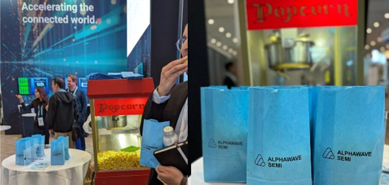
Bringing people together, one bag at a time!
Of course, hot popcorn was an enticing hit… irresistibly luring attendees to us in droves!
Bringing people together, one bag at a time!
Forward-thinking Perspectives: Inspire and Influence
A significant number of DAC attendees gathered to listen to Alphawave Semi’s Mohit Gupta and Clint Walker knowledge-share with unrivaled perspectives! Participating in panel discussions and giving presentations on hot topics including “The Industry 4.0 Revolution of Semiconductor Design” and “Chiplet and Die-to-Die (D2D) Interface Interoperability – How to Accelerate the Path to an Open Ecosystem”, Mohit and Clint really know how to engage and keep people listening intently!
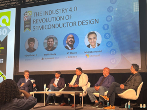 “In this new fast-moving generation of computing, custom silicon plays a major role, and that’s why high-speed data connectivity is so important. In older systems, power was only important for battery, now power has the main stage for systems design. The future of heterogeneous computing is chiplets!” -Mohit Gupta, SVP & GM, IP and Custom Silicon
“Two of the key technologies to enable chiplets are UCIe and advanced packaging. With these, a robust ecosystem of chiplets will help reduce costs by 35% and reduce time to market”. -Clint Walker, VP Marketing
Fostering understanding to ignite dynamic solutions for rapid evolution
We’re all about accelerating data transfer and transmission speeds with low power/latency. Our experts delighted large audiences with live captivating demos and stimulating discussions, while skillfully addressing inquiries and providing insightful answers! We’re the first company to announce UCIe PHY IP supporting faster die-to-die data rates of 24Gbps per lane, delivering bandwidth of 7.9 Terabits per second over a tight space of a mm of a chip beachfront. Not surprisingly, Alphawave Semi is on the forefront of keeping up with industry standards!
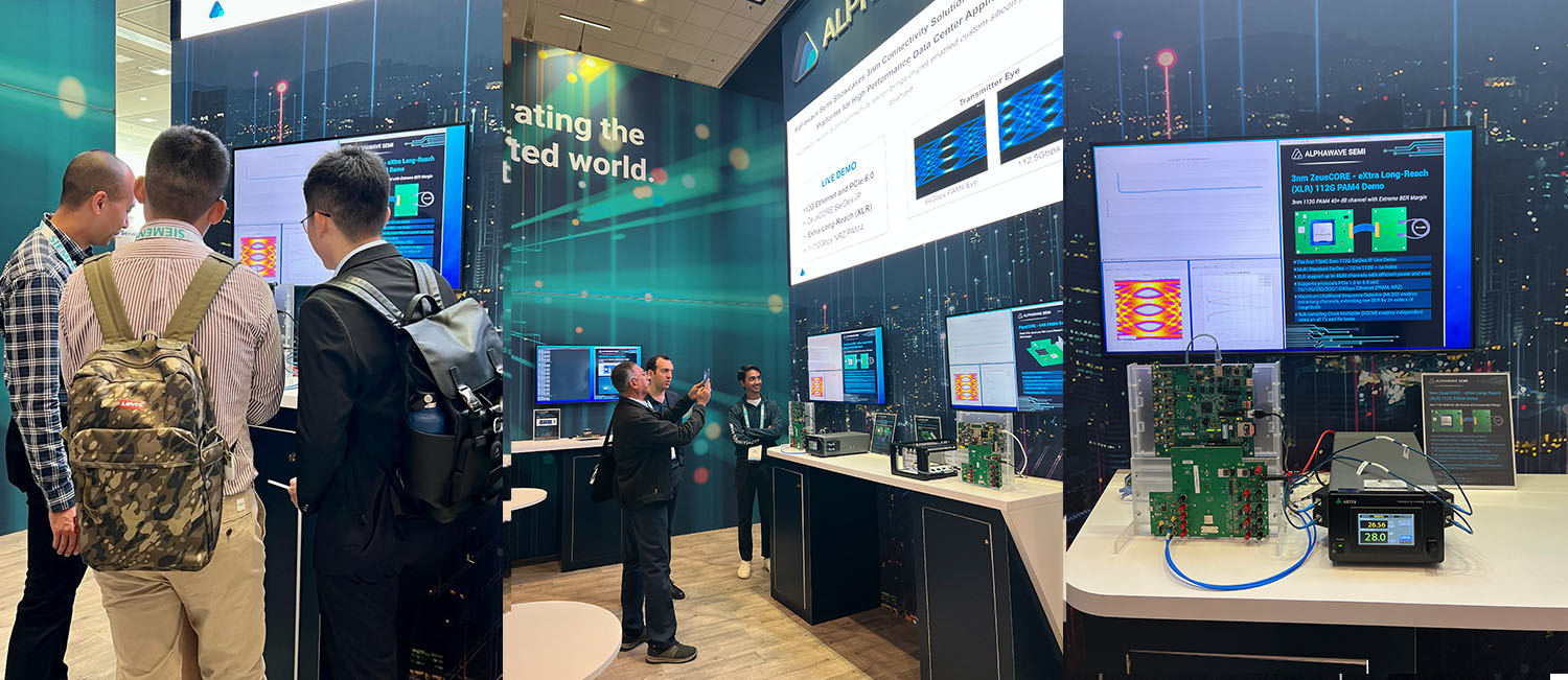
Each demo presented prominent key features and function elements
PipeCORE – 64G PAM4 Gen6 PAM4 PCIe Gen6 over Max Loss Channel with Extreme BER Margin
- Low Power Architecture
- Robust Training
3nm ZeusCORE – eXtra Long-Reach (XLR) 112G PAM4 3nm 112G PAM4 40+ dB channel with Extreme BER Margin
- The first TSMC 3nm 112G SerDes XLR IP Live Demo
- Multi Standard SerDes – 1G to 112G – no holes
AresCORE 16G D2D for chiplets in InFO_oS 2.5D package InFO_oS transmitting at 16Gbps D2D per lane with resulting received eye diagram
- Enables 2Tbps per module at extremely low power and latency
- Proprietary architecture reduces I/O complexity while saving power
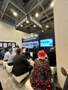
DAC 2023 was a spectacular show for Alphawave Semi. We look forward to seeing you at DAC 2024! 7.10.2023 – Alphawave Semi spearheads chiplet-based custom silicon for generative AI and data Center Workloads with Successful 3nm Tapeouts of HBM3 and UCIe IP. Alphawave Semi announced two successful tapeouts on TSMC’s most advanced 3nm process tailored for hyperscaler and data infrastructure customers. With increasing demands for more compute, memory bandwidth, I/O speeds, and energy efficiency, 3nm process technology paves the way for a new generation of chiplet-enabled silicon platforms. To effectively handle the exponential surge in data generated by AI, it’s crucial to develop advanced, able and efficient chips. Impressively, Alphawave Semi is the first company to announce UCIe PHY IP supporting faster die-to-die data rates! Read our full press release here: 6.14.2023 – Alphawave Semi Expands Collaboration with Samsung, adds 3nm Connectivity IP to Meet Accelerated AI and Data Center Demand. Alphawave Semi announces the expansion of its ongoing collaboration with Samsung to include the 3nm process node. To keep pace with the rapidly growing demands of data-intensive applications, Samsung Foundry platform customers now benefit from Alphawave Semi’s most advanced high performance connectivity IP and chiplet technologies, including 112 Gigabits-per-second (Gbps) Ethernet and PCI Express Gen6/CXL 3.0, interfaces to build the complex systems-on-a-chip (SoCs). Alphawave Semi unleashes unprecedented performance to power next generation AI and data centers! Read our full press release here: We highly value your continued support and enthusiasm. If you have any further questions or need additional information, please feel free to reach out to us at info@awavesemi.com Visit us at: www.awavesemi.com
