Alphawave Semi Elevates AI with Cutting-Edge HBM4 Technology
As generative AI and machine learning technologies continue to advance and scale within data centers, overcoming memory bandwidth and capacity limitations becomes crucial for developing more sophisticated large language models (LLMs). High Bandwidth Memory (HBM) has emerged as the preferred solution due to its efficient design, offering scalable and enhanced performance, vital for future AI advancements. HBM’s architecture allows for stacking to increase memory capacity and bandwidth, facilitating the creation of more complex LLMs. Modern AI silicon incorporates GPUs and accelerators, equipped with on-package HBM memory and cutting-edge connectivity SerDes, often featuring high-speed I/O options like 112G/224G Ethernet or 64G/128G PCIe, to boost performance.
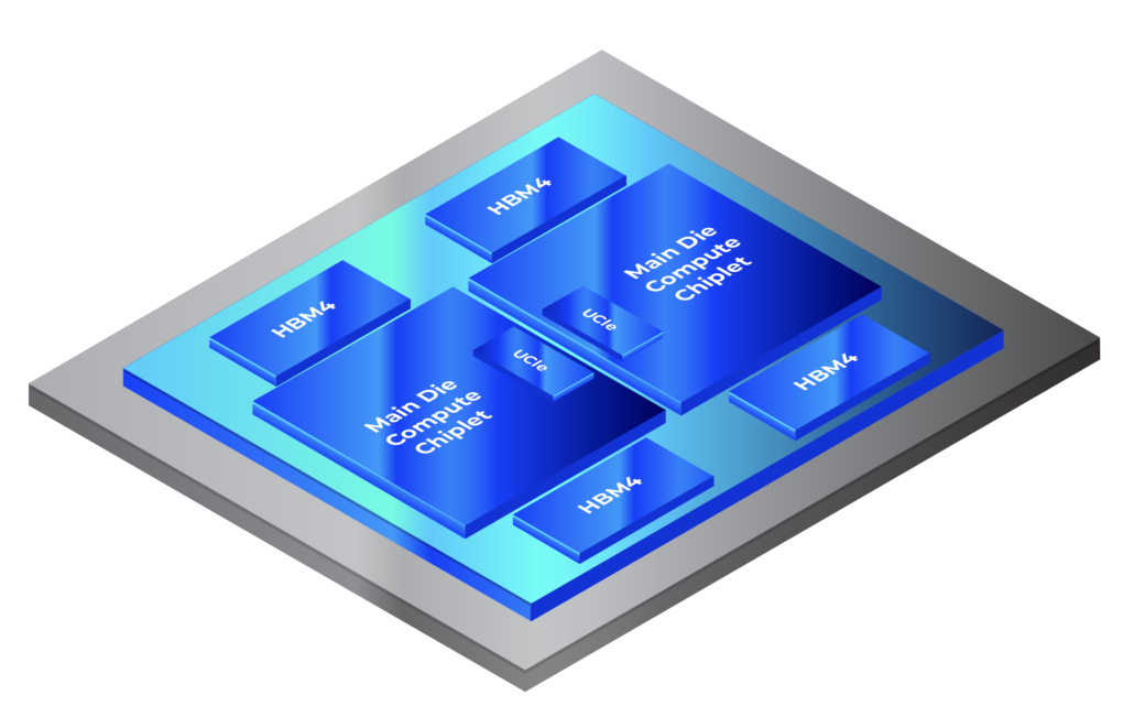
HBM4 Compute Chiplet Subsystem
Transitioning to HBM4 architecture
As the progression of HBM memory technology advances, each generation has seen an increase in data rates per pin. However, the transition from HBM3 to HBM4 marks a shift to a lower data rate per pin, from 9.2 Gbps with HBM3’s 1024-bit interface, to 6 Gbps with HBM4’s doubled interface width of 2048 bits. This change allows for a boost in aggregate bandwidth despite the initial drop in pin speed. Notably, HBM4 retains the same shoreline width as its predecessor, but this increase in density brings greater crosstalk challenges and complex issues regarding future data rate enhancements for HBM4 and HBM4E DRAMs.
System Level Analysis of HBM4
Alphawave Semi is advancing from its existing HBM3 framework to a more robust HBM4 architecture by capitalizing on its expertise in advanced packaging, signal and power integrity, and sophisticated silicon design. The company is meticulously evaluating various CoWoS interposer configurations, EMIB, and bridge interconnects, alongside packaging technologies provided by OSATs like ASE. These assessments are critical for optimizing dense routing while sustaining high data rates, which are essential for the performance demands of next-generation systems. Alphawave Semi has extensively reviewed channel parameters for traditional CoWoS-S silicon interposers, CoWoS-R redistribution layers, and EMIB, to identify the most efficient layouts for interposers, redistribution layers, or bridge interconnects, thereby maximizing performance and efficiency in an HBM4 subsystem.
The creation of an HBM subsystem encompasses the co-optimization of the memory IP, the channel, and the DRAM device, each integral to achieving peak combined performance that must be precisely calibrated for optimal operation.
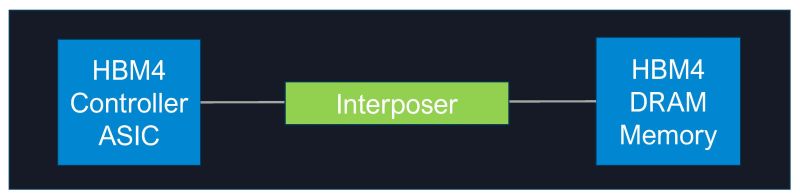
System Simulation Components
Utilizing 3D modeling tools to derive frequency responses through S-parameter models enables precise identification of critical channel parameters such as characteristic impedance, insertion loss, return loss, and crosstalk. This thorough analysis affords a deep understanding of the channel’s performance traits under various operational conditions, facilitating accurate forecasts of the link’s performance and data eye opening, which are vital for maintaining signal integrity. This method has been applied to assess multiple interposer layouts, significantly boosting the efficiency and dependability of the HBM subsystem.
Equalization
At the system level, eye simulations of the IBIS-AMI model for both the PHY and DRAM have facilitated examinations of signal quality throughout the HBM4 channel. This analysis is instrumental in optimizing the signal transmission and ensuring robust performance across the memory subsystem.
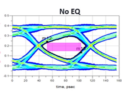
HBM4 Read Mode with No Equalization
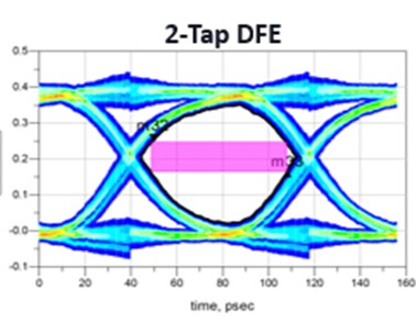
HBM4 Read Mode with 2-Tap DFE
By analyzing key channel parameters that contribute to eye closure, the team at Alphawave Semi was able to determine and quantify the factors that impact signal integrity. The I/O architecture was optimized to enhance data transfer and communication among components. The team investigated DFE equalization techniques to maximize eye openings—determined by eye height and width—to effectively counteract vertical and horizontal noise sources like jitter, without compromising system performance.
Ongoing iterative studies on signal and power integrity (SI/PI) and routing feasibility helped refine channel parameters, improving simulated data eye diagrams. A jitter decomposition analysis allowed the team to identify additional system margins for achieving higher data rates. Equalization techniques were finely tuned to offset any remaining signal degradation, thus preserving the integrity of the data as it moves across the interposer.
Interposer Design
As System-in-Package (SiP) designs grow in complexity with an increased size and component count, the challenges in package design and layout amplify, constrained by limited shoreline available for routing. Increased signal loss is likely as the channel reach extends from the PHY to the DRAM over longer interposer routing. The optimal interposer layout was determined by assessing critical channel parameters such as insertion loss, return loss, Intersymbol Interference (ISI), and crosstalk. Signal and ground trace widths and their spacing were analyzed using 2D and 3D extraction tools, leading to an optimized model that integrates microbump connections to signal traces, encompassing various interconnect layers and via connections. An iterative approach refined the density of ground and signal routing patterns to effectively shield against crosstalk between layers.
The interposer’s stack-up layers for signals, power, and decoupling capacitors underwent comprehensive evaluations for both CoWoS-S and CoWoS-R technologies in preparation for the transition to HBM4. This included detailed analyses of signal layer stack-ups, ground trace widths, vias, and the spacing between signal traces, enabling the optimization of the interposer layout to mitigate adverse effects and boost performance.
To achieve higher data rates, a jitter decomposition and analysis were performed on the interposer to budget for random jitter, power supply induced jitter, duty cycle distortion, and other factors, setting the necessary operating margins. The team engineered advanced silicon interposer layouts that provide excess margin, ensuring these configurations can support the elevated data rates required by future enhancements in HBM4 technology and varying operating conditions.
Future-Ready Performance with HBM4
Crosstalk was identified as the primary factor contributing to eye closure. Addressing this pivotal issue, Alphawave Semi’s design team devised innovative methods to minimize crosstalk, including the development of patent-pending structures tailored to reduce crosstalk within the interposer. These novel and advanced patent-pending solutions are crucial for preserving signal integrity and enhancing overall performance.
These enhancements ensure the interposer is equipped to handle the high data rates, signal density, and performance demands of HBM4. The layout designs not only tackle current challenges but also future-proof the interposer for upcoming generations of HBM, showcasing Alphawave Semi’s dedication to advancing technology and sustaining industry leadership.