Redefining XPU Memory for AI Data Centers Through Custom HBM4 - Part 1
Part 1: An overview of HBM
by Archana Cheruliyil
Principal Product Marketing Manager
This is the first of a three-part series from Alphawave Semi on HBM4 and gives an overview on the HBM standard. Part 2 will provide insights on HBM implementation challenges, and part 3 will introduce the concept of a custom HBM implementation.
Relentless Growth in Data Consumption
Recent advances in deep learning have had a transformative effect on artificial intelligence (AI) and the ever-increasing volume of data and the introduction of transformer-based models, such as GPT, has revolutionized natural language understanding and generation leading to improvements in virtual assistants, chatbots and other natural-language processing (NLP) applications. Training transformer-based models requires enormous datasets and computational resources, so while these models open new opportunities for AI-driven insights across industries, they also create challenges around data management, storage, and processing.
The Memory Wall and How to Address It
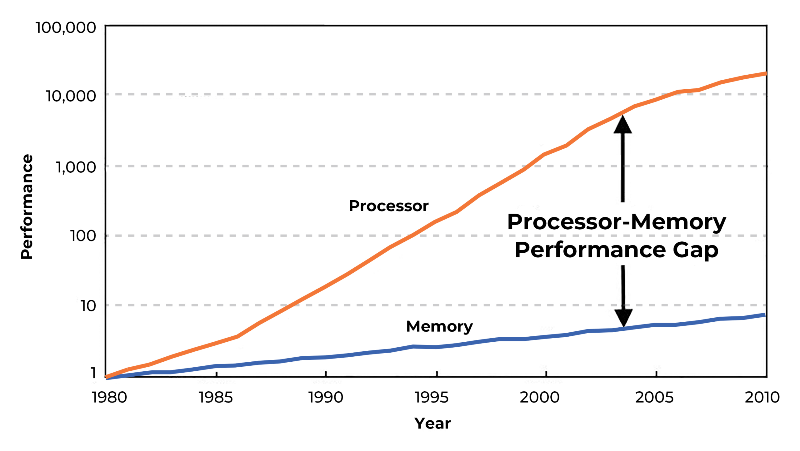
As AI models grow in both size and complexity, they generate and process increasingly massive datasets, leading to performance bottlenecks in memory systems. These memory-intensive operations strain the memory hierarchy, especially in high-throughput scenarios like training large neural networks. We see CPU processing power continue to increase, tracking with Moore's Law, however, memory access speed has not kept up at the same rate. Specialized AI hardware, while capable of extreme parallelism, is constrained by memory latency and bandwidth. This bottleneck, often referred to as the memory wall, can significantly affect overall system performance. To address these challenges and narrow the memory-performance gap, advancements are being explored in areas like 3D stacked memory technologies commonly known as High Bandwidth Memory (HBM).

Next Generation High Bandwidth Memory
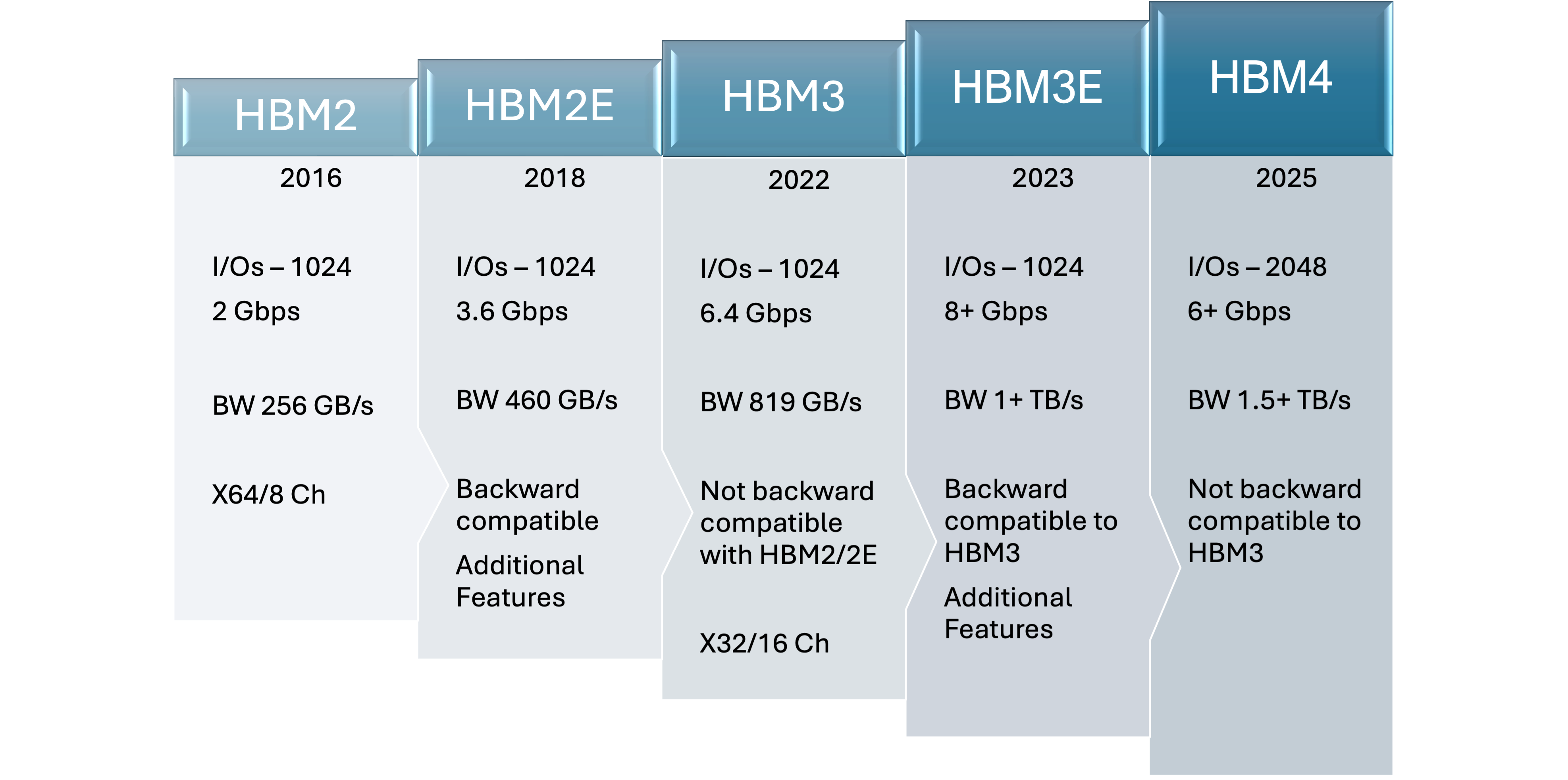
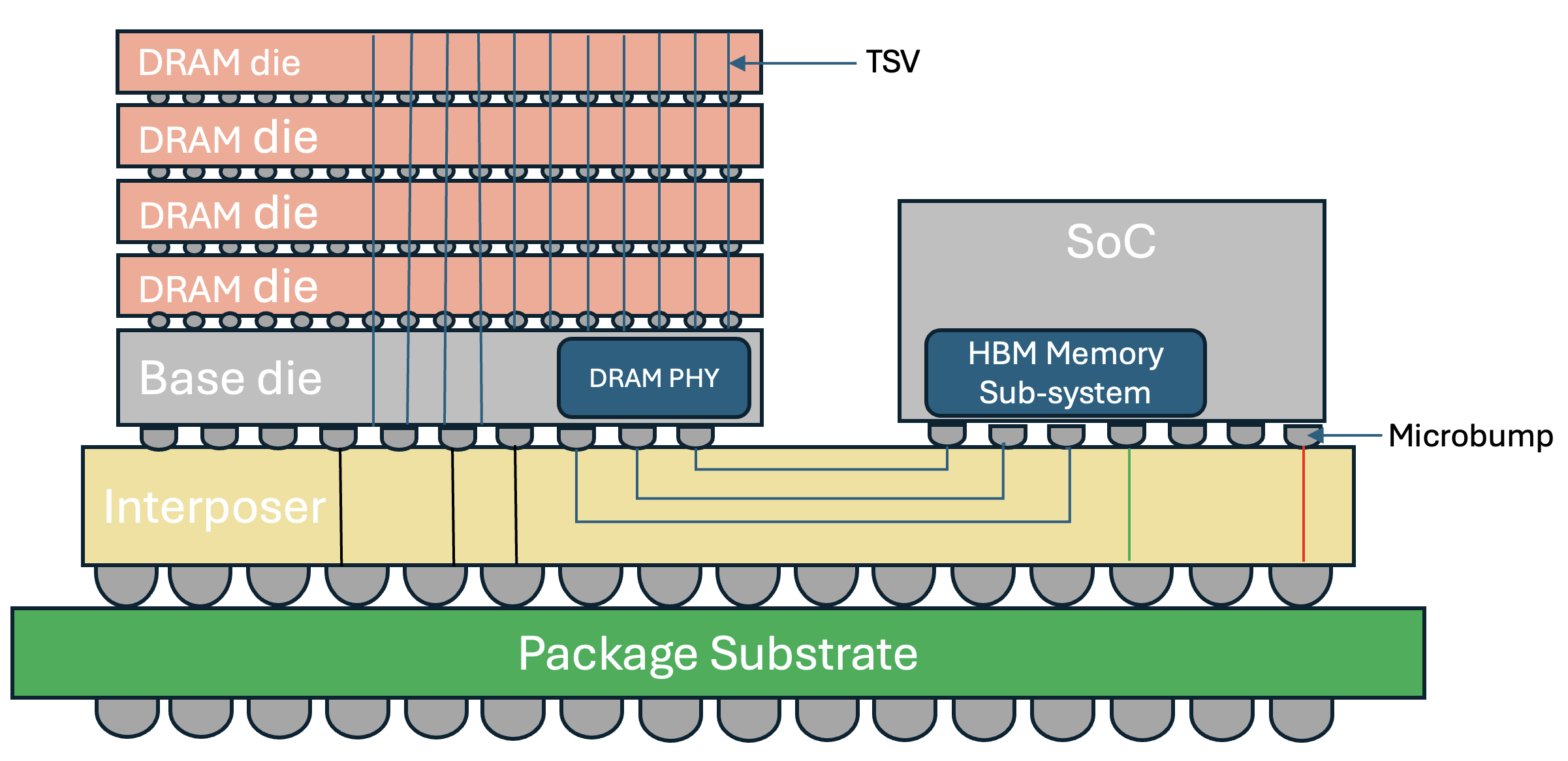
HBM utilizes a 3D-stacked architecture, where memory chips are vertically stacked and interconnected via Through-Silicon-Vias (TSVs). The stacked DRAM is connected to the processor dies through an interposer. This reduces the physical distance that data must travel and allows for higher data transfer rates with lower latency. Alphawave Semi’s complete HBM3E sub-system consisting of PHY, and controller offers a data rate of up to 9.6 Gbps, which enables a bandwidth of 1.2 TBps. The next generation HBM4 and HBM4E technologies will further address the needs of AI workloads by doubling the interface width to 2048-bits and Alphawave Semi’s memory IP roadmap will support this technology and deliver bandwidth up to 3 TBps.

Advantages of HBM
High Bandwidth – Using a wide memory interface bus allows massive bandwidth for data transfer between dies. This is particularly useful for parallel processing workloads such as those found in AI model training and deep learning.
Smaller Form Factor - HBM's 3D-stacked design offers a smaller footprint compared to traditional memory configurations. These stacks are then mounted next to the processor on a silicon or organic interposer, creating a highly compact memory system.
Low Power Consumption- HBM is also designed to consume less power than traditional memory, especially when delivering high bandwidth. Lower power consumption is a key factor in the design of modern computing hardware, particularly for AI systems that are often deployed at scale.
Reduced Latency – HBM offers lower latency compared to off-chip memory solutions such as DDR and GDDR. With recent investments in advanced packaging technologies such as 2.5D interposers and 3D stacking it allows more compact SoC designs suitable for heterogenous computing.
As AI continues to grow in complexity, the role of HBM will become increasingly important in unlocking the full potential of next-generation AI hardware.

Challenges of HBM
Manufacturing Complexity - HBM is built using a 3D-stacked architecture, and the precision required to manufacture TSVs and align multiple layers of memory die is much higher than for conventional memory. Additionally, HBM is typically mounted on a silicon interposer or organic interposer, which provides high-speed communication between the memory stack and the processor. This requires advanced photolithography techniques and precise die placement which adds to the overall complexity of manufacturing.
Thermal Management - Due to the stacked nature of HBM where several DRAM dies are placed on top of each other heat generated by the memory dies can accumulate within the stack. This creates a significant thermal challenge. Advanced cooling methods such as liquid cooling, thermal interface materials (TIMs), and integrated heat sinks are often required to mitigate thermal throttling.
Total Cost of Ownership – Since 2.5D interposers and 3D stacking technologies require advanced manufacturing techniques and achieving high yield could be quite challenging. Even a single defect in any of the stacked dies or interconnections can lead to failure of the entire HBM stack, reducing overall manufacturing yields and increasing costs.
Summary
HBM offers significant advantages for applications where performance and bandwidth are critical, and it remains one of the most viable solutions despite its cost and complexity. And as computational workloads evolve as a result of the explosive growth in AI and big data, new approaches to managing and accessing memory will be crucial to overcoming the memory bottleneck.
Alphawave Semi is uniquely positioned to provide a complete HBM4 sub-system solution consisting of area and power optimized PHY, highly configurable memory controller and a reference interposer design. Our industry-leading portfolio of connectivity IP solutions complement our HBM4 solutions to deliver the world's most advanced custom silicon devices, leveraging 2.5D and 3D advanced packaging.
Check out our 3-part blog series on HBM4.
- Part 1: Overview on the HBM standard
- Part 2: HBM implementation challenges
- Part 3: Custom HBM implementations
