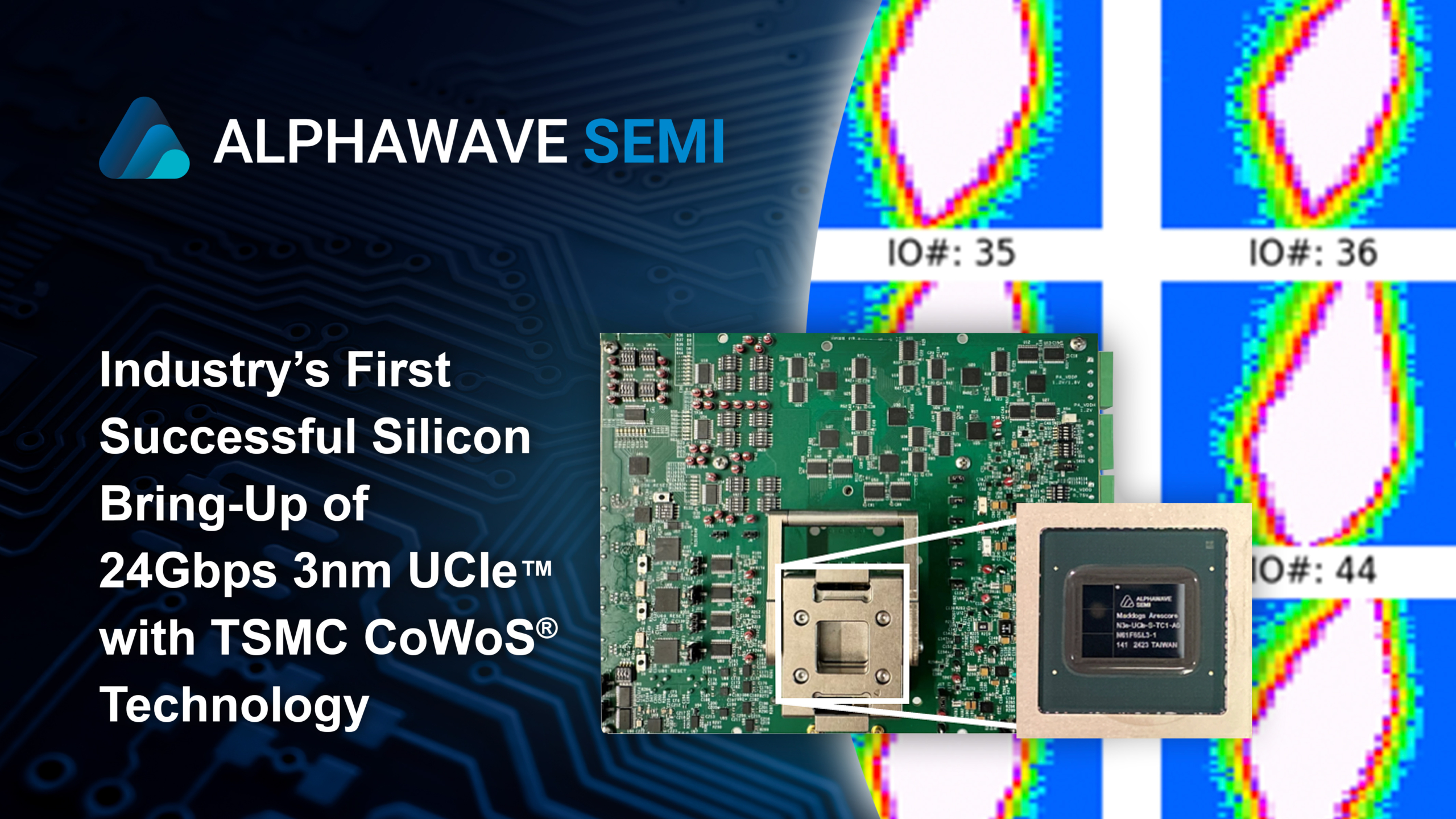
Alphawave Semi Launches Industry’s First 3nm UCIe IP with TSMC CoWoS Packaging
Multi-protocol subsystem IP provides 8 Tbps/mm bandwidth density with D2D data rate of 24 Gbps for hyperscaler, HPC and AI applications

LONDON, United Kingdom, and TORONTO, Canada – July 30, 2024 - Alphawave Semi (LSE: AWE), a global leader in high-speed connectivity and compute silicon for the world’s technology infrastructure, has launched the industry's first 3nm successful silicon bring-up of Universal Chiplet Interconnect Express (UCIe™) Die-to-Die (D2D) IP with TSMC’s Chip-on-Wafer-on-Substrate (CoWoS®) advanced packaging technology.
The complete PHY and Controller subsystem was developed in collaboration with TSMC and targets applications such as hyperscaler, high-performance computing (HPC) and artificial intelligence (AI).
Using the foundry’s CoWoS 2.5D silicon-interposer-based packaging, the fully integrated and highly configurable subsystem provides 8 Tbps/mm bandwidth density and reduces I/O complexity, power consumption and latency.
Supporting multiple protocols, including streaming, PCIe®, CXL™, AXI-4, AXI-S, CXS, and CHI, the IP enables interoperability across the chiplet ecosystem. It also integrates live per-lane health monitoring for enhanced robustness and enables operation at 24 Gbps to give the high bandwidth required for D2D connectivity.
“Achieving successful silicon bring-up of 3nm 24 Gbps UCIe subsystem with TSMC's advanced packaging is a significant milestone for Alphawave Semi and underscores the company's expertise in utilizing the TSMC 3DFabric™ ecosystem to deliver top-tier connectivity solutions,” said Mohit Gupta, Alphawave Semi’s SVP and GM, Custom Silicon and IP.
Gupta also stated the IP sets “a new benchmark in high-performance connectivity solutions.”
Alphawave Semi’s UCIe subsystem IP complies with the latest UCIe Specification Rev 1.1 and includes comprehensive testability and de-bug features such as JTAG, BIST, DFT, and Known Good Die (KGD) capabilities.
This launch follows Alphawave Semi’s February announcements stating its 3nm UCIe IP with standard packaging was silicon proven (link) and June’s release on the industry’s first multi-protocol chiplet (link).
For more information on Alphawave Semi, please visit http://awavesemi.com.
For more information on Alphawave Semi's UCIe IP, please visit https://awavesemi.com/silicon-ip/phy-ip/die-to-die-phy-ip/.
To learn more about Alphawave Semi's latest technology announcements, please visit https://awavesemi.com/company/press-releases/.
About Alphawave Semi
Alphawave Semi is a global leader in high-speed connectivity and compute silicon for the world's technology infrastructure. Faced with the exponential growth of data, Alphawave Semi's technology services a critical need: enabling data to travel faster, more reliably, and with higher performance at lower power. We are a vertically integrated semiconductor company, and our IP, custom silicon, and connectivity products are deployed by global tier-one customers in data centres, compute, networking, AI, 5G, autonomous vehicles, and storage. Founded in 2017 by an expert technical team with a proven track record in licensing semiconductor IP, our mission is to accelerate the critical data infrastructure at the heart of our digital world. To find out more about Alphawave Semi, visit: awavesemi.com.
Alphawave Semi and the Alphawave Semi logo are trademarks of Alphawave IP Group plc. All rights reserved.
Media Contact:
Claudia Cano-Manuel
Grand Bridges Marketing Limited
press@awavesemi.com
+44 7562 182327


