Redefining XPU Memory for AI Data Centers Through Custom HBM4 - Part 2
Part 2: HBM implementation challenges
by Archana Cheruliyil
Principal Product Marketing Manager
This is the second in a three-part series from Alphawave Semi on HBM4 and gives insights into HBM implementation challenges. Click here for part 1, for an overview on HBM, and in part 3, we will introduce details of a custom HBM implementation.
Implementing a 2.5D System-in-Package (SiP) with High Bandwidth Memory (HBM) is a complex process that spans across architecture definition, designing a highly reliable Interposer channel and robust testing of the entire data path including system level validation. Here is a breakdown of the key elements and considerations involved in implementing a 2.5D HBM design.
Advanced Design and Architecture Planning
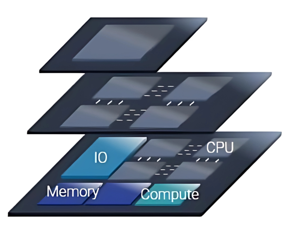
Determining the necessary bandwidth, latency and power requirements are important to plan overall system architecture. A monolithic chip can also be disaggregated to smaller specialized modules called chiplets to handle specific functions within the system. This approach can provide enhanced design flexibility, power efficiency, yield and overall scalability.

Interposer Design
The interposer can be either silicon or organic material and supports multiple metal layers to handle high-density routing between the HBM stacks and compute die. HBM4 will build upon improvements seen in HBM3E and aims to push data rates, energy efficiency and memory density further. With the interface width doubled (to 2048 bits), but with the HBM4 memory shoreline remaining the same as HBM3E, the primary challenge is how to manage the denser I/O routing in the PHY as well as the interposer. The layout should ensure careful signal routing, power distribution, and grounding to minimize crosstalk and losses through the channel to meet the HBM4E specifications. Alphawave Semi is implementing a test vehicle with HBM4E memory sub-system, interposer, package and board designed in-house to study the entire data path signal integrity on a leading-edge silicon node.
Signal Integrity (SI) and Power Integrity (PI) Analysis
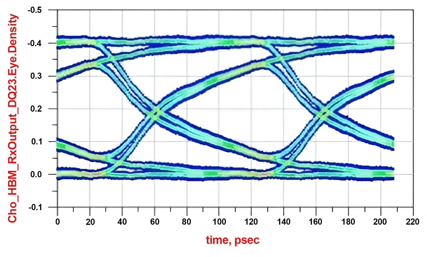
To prevent signal degradation at HBM4E data rates, Alphawave Semi is implementing techniques like impedance matching, shielding and measures to ensure minimal crosstalk between adjacent traces. The interposer is characterized for insertion loss (IL), reflection loss RL), power sum crosstalk (PSXT) and insertion loss to crosstalk ratio (ICR) to characterize the channel and ensure we meet the requirements of next generation HBM4E technology. Additionally, to achieve peak performance we are also upgrading the I/O architecture to include equalization techniques that ensures a maximum EYE opening through the data path channel.

Simulated WRITE EYE Diagram
The power delivery network also requires careful planning to determine decoupling capacitors, low impedance paths and dedicated power planes for critical sensitive signals. The noise contribution from all components including motherboard, package, interposer and silicon die needs to be considered in determining the target impedance of the power delivery network.
System Level Testing and Validation
Extensive SI-PI testing ensures the HBM package meets jitter and power specifications. Decomposing interposer-induced jitter into ISI, crosstalk, and rise-fall time degradation help to identify the dominant channel parameter affecting EYE closure and aids better layout and I/O architecture optimization.
System level testing of all components in the data path is critical to ensuring that assembled package meets the performance specifications set forth in the design phase. A comprehensive test suite which includes DFT-enabled design is also critical for early diagnostics to achieve high yield. Alphawave Semi supports a full range of DFT standards and functions across all major vendors and specialized EDA tools.

System Level Testing Components
Summary
While providing several benefits in achieving better performance and lower latency, HBM4 systems raise some complex technical challenges in architecture, interposer design, SI/PI analyses, test and validation. Alphawave Semi is well placed to overcoming these challenges to create industry-leading, high-performance, high-reliability HBM4 implementations for AI and data center applications. The critical need for more innovative memory solutions to keep pace with the data revolution is pushing the boundaries of what computational systems can do. A custom implementation of HBM4 allowing for greater integration with compute dies and custom logic, can be a performance differentiator justifying its complexity.
Check out our 3-part blog series on HBM4.
- Part 1: Overview on the HBM standard
- Part 2: HBM implementation challenges
- Part 3: Custom HBM implementations
