Unleashing AI Potential Through Advanced Chiplet Architectures
Tony Chan Carusone, CTO, Alphawave Semi
The rapid proliferation of machine-generated data is driving unprecedented demand for scalable AI infrastructure, placing extreme pressure on compute and connectivity within data centers. As the power requirements and carbon footprint of AI workloads rise, there is a critical need for efficient, high-performance hardware solutions to meet growing demands. Traditional monolithic ICs will not scale. Thus, chiplet architectures are playing a critical role in scaling AI.
Combining chiplets via low-latency and high-bandwidth connections across modular, custom components facilitates performance growth beyond the reticle limit. Connectivity standards such as UCIe enable seamless inter-die communication. Chiplets also support AI scale-up and scale-out. Even distributed AI across multiple sites benefits from chiplet architectures.
Harnessing the chiplet ecosystem to design flexible, interoperable compute and connectivity within a single package optimized for workloads is the only way to sustainably scale AI.
Data is proliferating
Machine generated data is proliferating like never before. The size of the data sphere will reach 181 billion terabytes (181 ZB) next year and the need to scale AI has accelerated new and upgraded data center infrastructure. However, processing isn’t the only limit – improvements in connectivity will also be critical in scaling AI.
A decade ago, data was primarily generated by people interacting with technology, and its growth was linear. With autonomous sensor and video data, financial data and yet more data produced by analyzing other data, the growth became exponential.
This is driving a focus on AI to parse all this data. Compute infrastructure is being pushed to the absolute limit imposed by the performance of a single full reticle-sized monolithic die. Hardware cost is a significant concern since deploying AI at scale may require, for example, 8 GPUs per server across 20,000 servers at a cost of around $4 billion. Energy is also a limiting factor representing millions of dollars in operational costs. Moreover, individual training runs are estimated to generate 500 tons of CO2 presenting environmental costs.
AI is driving power consumption
Although computing power consumption has been a growing concern for a while, AI is accelerating the trend as AI training demands large chips operate with high activity, continuously for weeks, or even months at a time.
According to the IEA electricity consumption from data centers is expected to reach 1,000 TWh within the next two years. A Goldman Sachs analysis suggests that by 2030, the US alone will reach this figure, that the data center’s share of power will rise from 2% in 2020 to 8% in 2030, with virtually all acceleration in electricity caused by AI.
If we assume the US’s mix of energy sources remains the same, then this 1,000 TWh will produces 389.8 metric megatons of CO2.
In many locations, data center consumption is a huge portion of total demand. In Ireland, it is expected to be 30% within a couple of years. Projections forecast that by 2026, global AI usage will consume more electricity than all bar five countries – Japan, Russia, India, the US and China.
Chips such as Nvidia’s H100 GPU consumes more energy than previous devices and, due to the cost, will not be idle for long – unlike traditional compute where overprovisioning addresses peak loads.
A bare H100 consumes 700W but, in a rack with networking and cooling, this can easily become 2kW. With Nvidia shipping 2 million GPUs annually the power consumption would rival that of a large US city – and later processors almost double the consumption.
Clearly, there must be a focus on low power design within AI to reduce consumption and benefit the planet.
The role of chiplets within AI computing
AI development started before the availability of dedicated hardware, with early applications running on server-grade machines. Hardware and software developments over two decades enhanced AI performance.
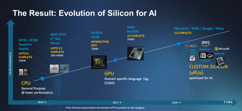
Fig 1: Silicon has rapidly evolved to support AI growth and with it a chiplet ecosystem has emerged to enable growth beyond the reticle limit.
Finally, the use of highly-parallel GPU architectures accelerated progress. Now, dedicated hardware is used to support the mathematical models for deep learning, including specific AI accelerator chips tailored to the data they must process.
Moving from teraFLOPS to petaFLOPS will require even more specialized hardware and with a low power consumption. It’s not just the AI accelerators that need this attention, it applies to devices such as CPUs and networking as well. The energy-efficient performance must come at a lower cost as hyperscalers require hundreds of thousands of these devices to continue scaling AI.
The pace of AI development now demands new custom silicon chips every 12 months, but the design, verification and fabrication cycle of these custom devices is 18-24 months. Thus, chiplets are the only viable solution to maintain the annual cadence of hardware upgrades that AI scaling demands.
To understand the benefits of chiplet architectures, consider a monolithic IC implementation where all the logic and I/O are on a single die. Implementing such a large ASIC monolithically implies all of it must be in a single technology. So, for example, DRAM must be outside the package. Additionally, the advanced CMOS die is burdened with analog/mixed-signal circuits that take away from the area available for logic and embedded memory. Such designs will be limited by the maximum die size and, approaching limit will reduce yield, pushing costs higher. The integration of complex IP to make a single chip increases the time required for design and verification, and if that timeline is rushed, risk increases.
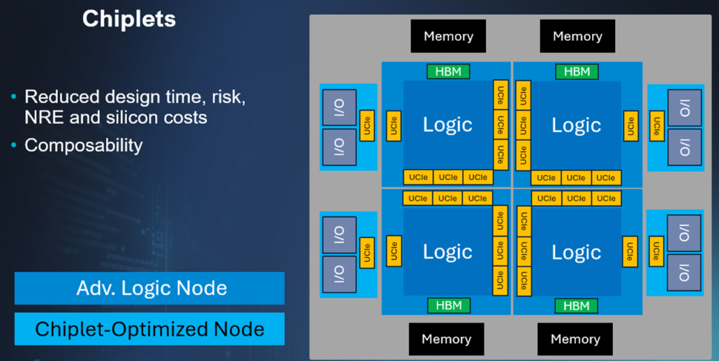
Fig 2: Chiplets deliver significant benefits in designing for advanced AI.
However, with chiplets, performance, bandwidth and lower cost are realized by putting the latest processors on sub-3nm tiles, interconnected with low-latency die-to-die interfaces. I/O transceivers for Ethernet and PCIe can be moved to separate I/O tiles, which can be implemented in whatever process technology best suits those circuits.
All tiles can be separately pre-designed and validated in parallel, lowering the overall design cycle time. Developing chiplets in this way can increase the compute power for a single part while increasing yield – and lowering cost by up to 40% – due to the use of smaller dies.
Scaling this across millions of AI accelerators within data centers leads to incredible savings. Reasonable estimates put this in the region of billions of dollars for hardware and hundreds of gigawatts of power. With these clear benefits, chiplets are being used for virtually all large compute & networking chips entering development today.
UCIe for die-to-die connectivity
The key to successful chiplet-based designs is low-latency, low-power interconnect between tiles, allowing the whole system to perform as a single chip.
The UCIe die-to-die interconnection standard is proving crucial in the ecosystem. It is an open standard allowing developers to choose the optimum elements for each part of the SoC. It offers 10+Tbps per mm of die edge at energy consumptions below 0.5 picojoules per bit, with a latency of very few clock cycles. To achieve this combination of bandwidth density and low power, attention must be paid to maintain signal integrity, power integrity, and high-performance clocking across the interface.
Scaling AI with connectivity
AI is scaling along two dimensions. Scaling up involves adding more resources per computer (i.e. more accelerators per server) while ‘scaling out’ adds more servers to spread the workload. The scaling is happening in both directions simultaneously, while each individual AI accelerator is simultaneously becoming more powerful due to chiplet design. This is creating a dramatic increase in data processing and, thus, networking demands.
Traditional data center networks are evolving. As data rates increase, optical is replacing electrical in more links and active solutions (using retimers) are replacing passive solutions, yet there is increased focus on low power consumption and cost.
Machine learning AI clusters are connected by their own back-end networks allowing direct memory access that is isolated from traffic demands on the front-end network. The backend networks have specific requirements, including high sustained bandwidth due to the significant AI workloads running there. Scale up networks, in particular, require low latency which implies a flat hierarchy. Robustness and reliability of the links are crucial as packet losses on a single link can bottleneck the whole workload.
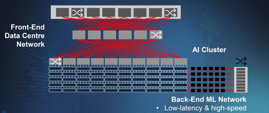
Fig 3: AI clusters sit on a high speed, low-latency back-end network (top) and distributed AI (bottom) delivers privacy but required high speed broadband connectivity.
Interconnectivity in the modern data center
A modern server shares a lot with a typical PC, containing one or more CPUs, memory, storage and a (front-end) network interface. The primary interconnect will usually be PCIe between the CPU and its peripherals, Ethernet to other compute nodes, and DDR for the memory.
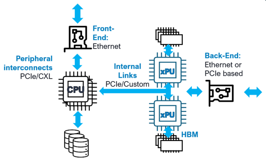
Fig 4: AI compute nodes add xPU capability and connect to the back-end network.
An AI compute node is more complex but will include many similar parts. Powerful xPUs are added with significant quantities of their own dedicated memory. To perform the most complex machine learning/AI tasks, many xPUs will need to collaborate and have seamless access to each other’s memory. This requires a back-end network interface to connect to the ML network.
Thus, there is a suite of connectivity technologies that enable AI comprising PCIe, Ethernet, HBM and UCIe. Whereas Ethernet is always used for the front-end network, the back-end network may include customized Ethernet and/or PCIe interfaces that reduce latency and/or improve reliability. Connections to the CPU and storage leverage PCIe, and possibly CXL, interfaces. The internal links between chiplets in the CPU and xPU can use UCIe while the GPU connects to memory via HBM.
AI scaling is also impacting the connections to memory and storage. On average, a third of memory in data centers sits unused, yet a third of infrastructure spend is here – meaning over 10% of the overall spend is wasted. Sharing storage in centralized pools allows for its more efficient use, affording cost savings of 30%. Such disaggregated architectures require low latency connectivity with sufficient reach. As distances exceed a few meters, optics are likely to be required.
Scaling up and out is allowing 100’s thousands of xPUs to collaborate on workloads, but that increases connection lengths. Although passive copper solutions offers low cost and power consumption, it simply cannot deliver the required bandwidth, speed and reach for AI scaling. Thus, we see increased use of fiber optics.
Today, optical connectivity is typically established via pluggable modules in servers and switches. These transceivers are being re-architected for AI and benefitting from chiplet-based design. Leveraging silicon photonics and advanced packaging technologies, tighter integration can be achieved, delivering cost and power savings when integrating many parallel lanes of traffic.
Chiplet architectures also open the door co-packaged optics (CPO), offering the potential for optical connectivity right to the xPU and switch. Direct-drive CPO relies on high-performance DSP SerDes on the xPU or switch to handle both optical and electrical links. The use of chiplets allows the broadband analog amplifiers to be implemented separately in their own process technology alongside a photonic chiplet. Digital-drive CPUs use UCIe to connect to the optical I/O on a separate chiplet, requiring less space on the central logic tiles. With this approach, optical and/or electrical interface chiplets can be integrated to create the desired solution for each application. Moreover, digital-drive CPO allows for tremendous bandwidth density in the die-to-die interface to the logic tile. To allow all that bandwidth to escape the package, several approaches are being considered, such as the use of multiple wavelengths and/or dense fiber-attach methods along with dense transceiver circuit design.
Distributing AI
Another key trend is that AI is being distributed across sites that can be separated by kilometers creating new connectivity challenges. There are several motivations for this trend. Regional data centers are being located at “the edge,” close to end users to allow for a responsive experience. It’s also becoming desirable to spread large AI workloads across multiple facilities to form a single larger virtual data center. Distributed training is gaining momentum as it preserves privacy by training AI models without passing sensitive information between institutions. In this approach, models are trained locally and only model updates are shared with the server, without sharing sensitive data such as medical image analysis for healthcare AI, individual location data for autonomous vehicle training, or financial data for fraud detection.
Distributing data centers geographically requires new types of broadband connectivity. Coherent-Lite is seen as an enabler in this area. These transceivers implement coherent optical connectivity, previously developed for reaches exceeding 100km, with greatly reduced power consumption. Coherent-lite transceivers leverage chiplet design paradigms to achieve this, combing bare dies made with different fabrication technologies into a highly-integrated, low-power subsystem.
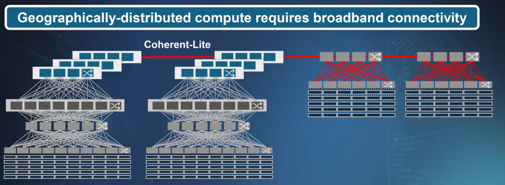

Fig 5: As AI moves to the edge to provide more responsive inference, data centers are becoming distributed (top). Distributed AI training allows for better data security and privacy (bottom). Both rely heavily on new connectivity technologies, including coherent-lite.
Enabling the chiplet ecosystem
To support AI scaling and foster the chiplet ecosystem, Alphawave Semi has developed UCIe IP across the world’s most advanced CMOS nodes along with a portfolio of reconfigurable, customizable, and interoperable chiplets.
It includes the industry’s first off-the-shelf multi-protocol I/O connectivity chiplet on TSMC’s 7nm process, integrating Ethernet, PCIe, CXL, and UCIe standards to provide high-bandwidth, low-power connectivity for AI and HPC applications. This chiplet, offering up to 1.6 Tbps bandwidth across 16 lanes, enables flexible, scalable system designs by allowing customers to mix and match with existing hardware ecosystems without extensive customization.
Alphawave Semi has also partnered with Arm to develop a high-performance compute chiplet using Arm Neoverse Compute Subsystems (CSS) for AI, HPC, data center, and 5G/6G networking. This chiplet integrates Alphawave’s advanced connectivity IP, including PCIe Gen 6.0/7.0, UCIe, and high-speed Ethernet, supporting scalable and efficient system-on-chip (SoC) solutions tailored to complex digital infrastructure needs.
These developments underscore Alphawave Semi’s commitment to advancing a robust chiplet ecosystem for high-performance AI and data center infrastructure.
Summary
AI has redefined data center infrastructure compute and connectivity. Chiplets enable the custom silicon solutions that are optimized for AI workloads and are essential to affordably scale performance and keep power consumption manageable. Chiplets also enable hardware developers to use trusted, proven silicon IP to get to market more quickly and meet the cadence of AI hardware design cycles.
