Custom silicon offers significant advantages for Artificial Intelligence (AI)-enabled applications, compared to using off-the-shelf general-purpose chips. Here are some key benefits:
Performance:
- Targeted optimization: Custom silicon can be precisely tailored to the specific needs of an AI algorithm or application, leading to significant performance improvements. This can include faster processing speeds, lower latency, and higher accuracy.
- Hardware-software co-design: By designing both the hardware and software together, you can create a tightly integrated system that optimizes performance and efficiency.
Power efficiency:
- Reduced energy consumption: Custom silicon can be designed to be more power-efficient than general-purpose chips, which is crucial for battery-powered devices and for reducing data center energy costs.
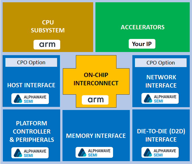
- Specialized accelerators: Dedicated hardware accelerators can be implemented for specific AI tasks, like matrix multiplication or convolution, to significantly boost performance while reducing energy consumption.
Flexibility and innovation:
- Unique features: Custom silicon allows you to implement unique features and functionalities that are not available in off-the-shelf chips, giving you a competitive edge.
- Specialized innovation: You can differentiate your system and accelerate your AI architecture with hardware-based acceleration.
Other advantages:
- Cost-effectiveness: While the initial development cost of custom silicon can be high, it can be more cost-effective than using many general-purpose chips in the long run, especially for high-volume applications.
- Security: Custom silicon can be designed with enhanced security features, such as hardware encryption and tamper resistance, which is important for protecting sensitive data and algorithms.
Custom silicon can be a powerful tool for unlocking the full potential of AI-enabled applications.


