Unleashing Die-to-Die Connectivity with the Alphawave Semi 3nm 24Gbps UCIe Solution
Elevate the performance of your system with Alphawave Semi’s extremely low power, low latency UCIe subsystem
Die-to-die interconnects are the driving force behind the development of disaggregated systems. These interconnects are revolutionizing diverse domains such as data centers, edge computing, artificial intelligence/machine learning (AI/ML), autonomous systems, and high-performance computing (HPC); domains that have typically been addressed monolithically up to the breaking point of operating at the reticle limit. The demand is driven by the requirements of high throughput bandwidth, low latency, and low power in these applications. Advances in packaging technology are further enabling the adoption of heterogeneous systems with chiplets and known-good-die (KGD) assembly to create solutions that require the evolution of a new kind of interface popularly known as Die-to-Die (D2D) interfaces.
The critical building block that makes this innovation possible is UCIe, Universal Chiplet Interconnect Express. Alphawave Semi has been pioneering D2D technology to fulfill the demand of complex and growing market requirements. Alphawave Semi’s UCIe subsystem is an extremely low power, low latency, flexible and complete D2D solution. The solution is now silicon-ready, being demonstrated on the leading edge 3nm process node, and configured for standard and advanced package technologies.
Key highlights of the Alphawave Semi 3nm UCIe subsystem are:
- 24Gbps data-rate-per-lane
- Architecture is compliant with the latest UCIe Specification Revision 1.1
- Supports x16 or x32 Standard Package, and x32 or x64 Advanced Package
- Bit Error Rate (BER) Health Monitoring
- Highly configurable D2D controller that supports
- Streaming
- PCIe, CXL
- AXI-4, AXI-S
- CXS
- CHI
- Comprehensive testability with features for KGD (Known Good Die)
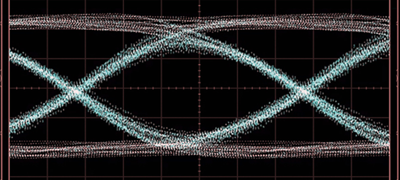
The 24Gbps eye diagram on the channel between the D2D interconnect is generated using PRBS generated patterns as shown below:
This new silicon proven 3nm UCIe subsystem expands Alphawave Semi’s leadership to the future of the robust and open chiplet ecosystem.
Chiplet Summit ’24 (February 6-8, 2024)
Visit the Alphawave Semi booth to see the 3nm 24Gbps UCIe demonstration.
Learn more about UCIe and the chiplet ecosystem at the following Chiplet Summit sessions:
![]()
Additional Resources
- Webinar: Achieving High Performance Compute with AI Chiplets Through UCIe Die-to-Die Interconnects - Alphawave Semi
- Press Release: Alphawave Semi Spearheads Chiplet-Based Custom Silicon for Generative AI and Data Center Workloads with Successful 3nm Tapeouts of HBM3 and UCIe IP
- Press Release: Alphawave Semi Elevates Chiplet-Powered Silicon Platforms for AI Compute through Arm Total Design
- White Paper: Will Chiplet Adoption Mimic IP Adoption?