UCIe for 1.6T Interconnects in Next-Gen I/O Chiplets for AI data centers
Letizia Giuliano, VP of IP Product Marketing & Management, Alphawave Semi
The rise of generative AI is pushing the limits of computing power and high-speed communication, posing serious challenges as it demands unprecedented workloads and resources. No single design can be optimized for the different classes of models – whether the focus is on compute, memory bandwidth, memory capacity, network bandwidth, latency sensitivity, or scale, all of which are affected by the choke point of interconnectivity in the data center.
Processing hardware is garnering attention because it enables faster processing of data, but arguably as important is the networking infrastructure and interconnectivity that enables the flow of data between processors, memory and storage. Without this, even the most advanced models can be slowed from data bottlenecks. Data from Meta suggests that more than a third of the time data spends in a data center is spent traveling from point to point. By preventing the data from being effectively processed, connectivity is choking the current network and slowing training tasks.
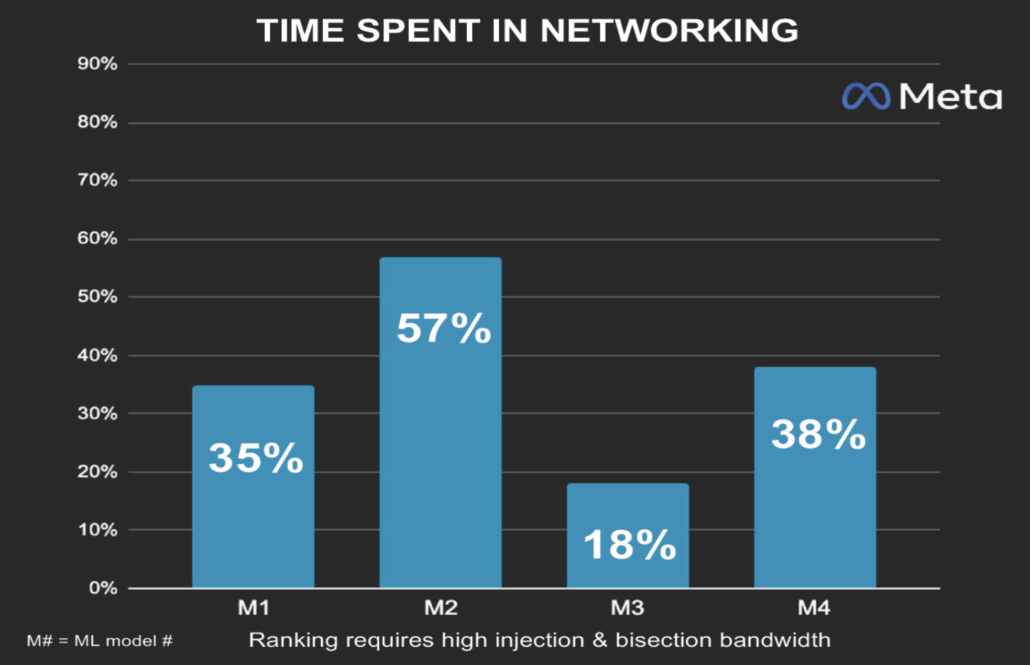
Fig 1: Data from Meta suggests more than a third of the time data spends in a data center is effectively wasted, moving from processor to processor across the network.
AI data centers
Infrastructure architecture for AI data centers requires a new design paradigm from that used in traditional data centers. Machine learning-accelerated clusters residing in the network’s back end, which handle AI’s large training workloads require high bandwidth traffic to move across the back-end network. Unlike the front-end network, where packet-by-packet handling is needed, this traffic (typically) moves in regular patterns and operate with high levels of activity.
There are steps to reduce latency, with fast access to other resources enabled by a flat hierarchy through limiting hops. This prevents compute from being underutilized, as the performance of AI networks can be bottlenecked by even one link with frequent packet loss. Optimizations in switching designs to be non-blocking, and network robustness are critical design considerations. These back-end ML networks allow AI processors to access each other’s memory seamlessly, as the dedicated network isolates the data from the vagaries of front-end network demands, which rise and fall with various priorities depending on the incoming compute request.
Connectivity in AI data centers
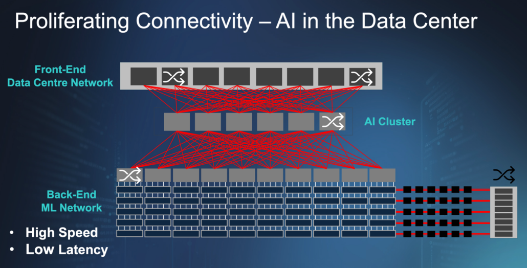
Focusing in on the AI cluster connectivity. As CPUs have taken a managing role in the proliferation of AI connectivity in the data center, a suite of several connectivity solutions is required to keep the XPUs networked together and enable the scale necessary to keep up with the latest models. Alphawave Semi offers industry leading solutions for all of these.
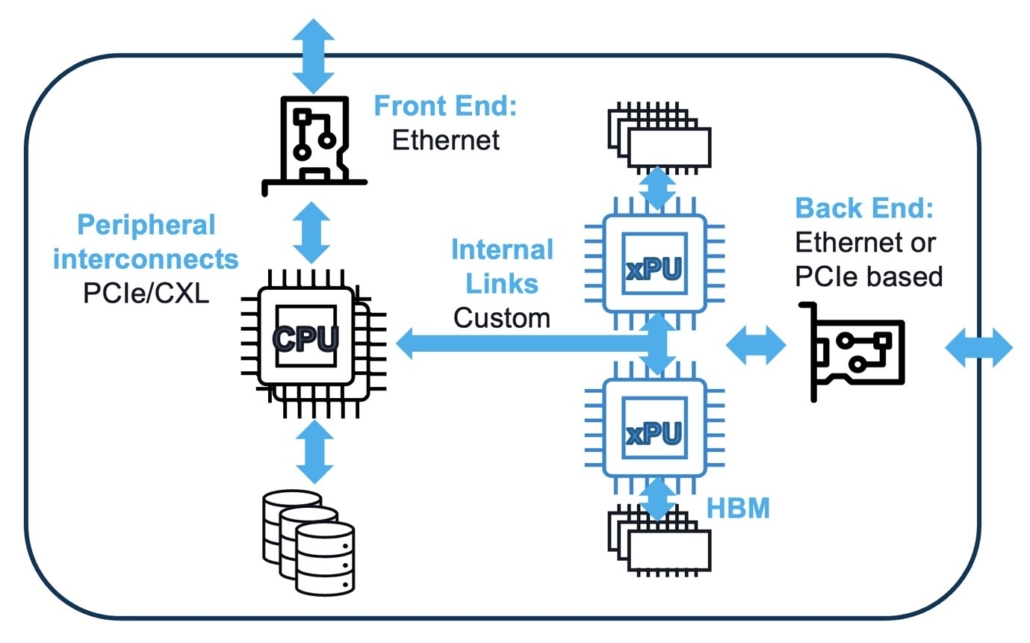
Fig 2: A simplified data center network displaying connectivity required.
The AI cluster connects to the front-end networks via Ethernet through a network interface card (NIC), which can go up to 112G/lane today; you will likely find the fastest speeds in the ethernet switches tying all of these NICs together, and 224G SerDes enabling 1.6T pluggables are coming soon with the P802.3dj standard.
Internal to the server, the PCIe is used to connect the CPU to the front-end NIC, the XPUs, and other peripherals, such as storage, with PCIe 5.0 used today, PCIe 6.0 to be deployed very soon, and not far off is PCIe 7.0 with the first revision of the specification set to be published in 2025. PCIe offers an intrinsically lower latency solution when compared to Ethernet for this aspect of AI connectivity, and the increased efficiency and uptime of compute and storage connections utilizing a PCIe PHY with either a PCIe or CXL layer on top to pool memory and storage resources of the network. This effectively makes the memory and storage look like one large resource, instead of many fragmented resources in practice.
The back-end network, where low latency and high speed are paramount, sees the proliferation of tailored connectivity MSAs. Ultra Accelerator Link (UALink) will be used as an alternative to other proprietary technologies to deliver highly parallelized connectivity to scale-up over 1000 XPUs together.
Within a server or compute rack, internal links between XPUs also use UALink (or another proprietary solution) with extremely dense I/O within the package to connect the compute die to memory.
Scaling network barriers
Scaling this model makes it increasingly difficult for monolithic SoCs to include all the necessary communication bandwidth plus the additional required functionalities without going past the reticle limits of the photolithographic equipment. Doing so introduces more defects as well as increasing wafer costs, ultimately reduces yields.
The alternative approach is to use a chiplet-based architecture. Unlike traditional monolithic SoCs, this unites small and specialized building blocks that have each been created on a process to specifically optimize for function, cost, power, etc. Chiplets can, in many ways, be thought of as an extension to the IP model, with the final SoC using chiplets from multiple vendors.
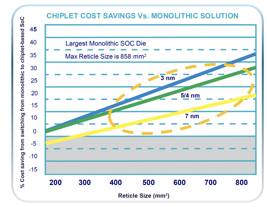
Fig 3: Moving to a chiplet design in 7, 5, and 3 nm can reduce the total cost of ownership – by more than 30 percent for the largest SoCs on advanced processes.
Having a smaller die size delivers greater yields and, due to the ability to reuse proven silicon, the model cuts NRE (non-recurring engineering) costs. Data also suggests that by using this model it is possible to reduce the power of the overall system somewhere between 25 and 50 percent.
Moving back to the data center, we can envision different types of I/O chiplets with different configurations of I/O connectivity. These would then be combined with memory chiplets for different types of memory subsystems, and compute chiplets developed for specific types of workloads or AI applications.
These are not the only market drivers behind a move to chiplet architectures, with advances in IC packaging technologies playing a crucial role. These include 2.5D silicon interposer, RDL interposer, embedded bridge, and 3D, where we see the deployment of hybrid bonding and technologies to enable a more stacked-die solution.
Industry standards on die-to-die interconnect protocols also play a key factor. Cross-supply-chain collaborations, like the MDI Alliance from Samsung and the 3DFabric™ Alliance from TSMC, are helping to simplify assembly and driven by the foundries.
1.6T
Monolithic SoC dies currently exceed the reticle die limit and have done so for more than five years. Before this limit was reached, it was possible to increase the die size and deliver increased bandwidth - larger die area equals more pins, but to continue this will become prohibitively expensive as one can no longer significantly increase the number of lanes around the chip or in the cable, and therefore cannot just add significantly more ports.
Another aspect to consider is thermal density on the front panel. There is a standard rack size used for data center infrastructure limited how much power and how deep and wide a typical rack server can be designed. Ultimately, the bandwidth per lane must be increased and move to a more scalable architecture.
For example, a 51.2 terabit switch in use (created via an aggregated 512-lane x 100G links), would benefit from increasing the data rates per link to the incoming 200G links. This enables the same bandwidth to be delivered with fewer links (256) and would move the SoC back below the reticle limit. Increases above 51.2 terabits could then be delivered by using a more scalable path (to 512 x 200G links) via a chiplet architecture.
The future AI SoC
Returning to the ‘traditional’ monolithic AI SoC, with its limited peak-connectivity anatomy, these are (typically) large chips designed on 2 and 3 nm process nodes. As discussed earlier, these include CPU cores, interconnect, memory, cache, and SRAMs, with a custom accelerator and security IP plus core-to-core, and logic-to-logic connectivity and a dedicated chip-to-chip link.
PCIe and Ethernet connectivity are key IP building blocks in the AI SoC that can be easily disaggregated. Doing so reduces the communication functions on a large AI SoC die to small I/O chiplet dies for use across different systems and applications. In such a chiplet-based SoC, the key connectivity IP for this will be PCIe/CXL, Ethernet, UCIe and HBM.
There are some drawbacks when implementing a chiplet architecture. There is a duplication of the same function on different dies; the same PHY and controller will likely be on both sides of a D2D link. This can impact power and area, as well as latency and it is vital to consider multiple factors when selecting the die-to-die interconnect in order to optimize the design.
Bandwidth density must be optimized to match the form factor and the package type being used, as well as cost. Additionally, power consumption must be a key design consideration with sub-pJ/bit being the target as each node looks to devote as much power to the compute and not to the interconnect.
These considerations make the UCIe protocol a key choice. Not only is it designed for the lowest possible latency, but also has a bandwidth density greater than 10 Tbps/mm, and a power consumption of 0.3 pJ/bit. In addition, the standard is highly robust and has full protocol stack definitions and platforms for interoperability.
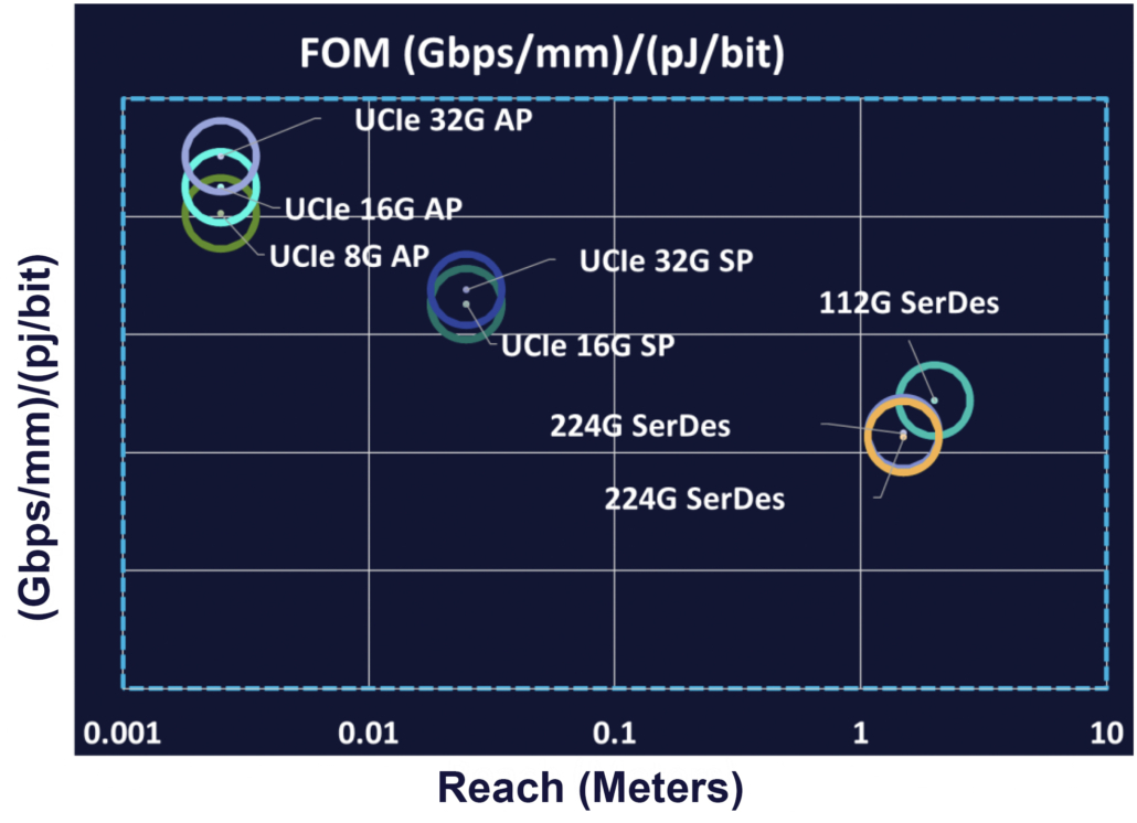
Fig 4: A comparison of chiplet die-to-die interconnect protocols in terms of energy efficiency and density.
As seen in figure 4 (above), the optimal die-to-die interconnect between chiplets in terms of shoreline bandwidth density (Gbps/mm per pJ/bit), is the UCIe parallel interface; chiplet designs powered by UCIe can enable 224G SerDes and the next generation of high radix use cases, such as switches.
The Future of AI Chiplets
AI workloads are set to grow in complexity and size, with the need for advanced silicon solutions increase in line with this.
Alphawave Semi is committed to leading this charge and our chiplets, which have been optimized for AI applications, from I/O to memory to compute are enabled by UCIe, in addition to a myriad of other high-performance interconnects.
In September 2024 Alphawave Semi announced the availability of the industry’s first silicon-proven UCIe subsystem on 3 nm processes, which is developed specifically for use in high-performance AI infrastructure. Alphawave Semi also launched a 1.2 Tbps connectivity chiplet for HBM3E subsystems (June 2024), taped out the first multi-protocol I/O chiplet for HPC and AI infrastructure and collaborated with Arm, Samsung and TSMC on AI and HPC chiplets using process nodes down to 2 nm. To round off these accomplishments, TSMC announced Alphawave Semi as its high-speed SerDes partner of the year in September 2024.
Modern data centers require scalability, power efficiency and flexibility and by driving innovation in chiplet-based design, advanced packaging, and interconnect technology, Alphawave Semi is leading the way for the next generation of AI-enabled data centers.
Further information on our chiplet offering is available here, and on our AresCORE UCIe die-to-die PHY IP is available here.
